
Speed and passion, quality first
To accelerate innovation and safeguard qualityOur end-to-end service is a highly collaborative and seamless' highway '
Date:2026-07-03
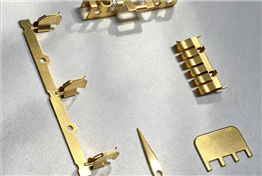
Many hardware engineers have encountered the same dilemma: even after installing metal shielding cans as designed, the finished product still fails EMC and RF anti-interference tests. In some cases, the interference issue becomes even worse than before the shielding can was installed. Drawing on our years of experience in precision stamping shielding can manufacturing and supporting customer projects, we have summarized 5 core high-frequency pitfalls that lead to such problems.
Poor Grounding Design Renders Shielding Cans Ineffective
For a shielding can to function properly, it must form a complete, low-impedance electrical connection with the PCB ground plane. Issues such as relying solely on single-point snap-fit grounding, poor contact of grounding shrapnels, and oxidized PCB grounding pads will prevent the shielding housing from forming an effective Faraday cage, allowing interference signals to radiate and leak through gaps. It is particularly important to note that more grounding points do not always equal better performance: high-frequency circuits require multi-point grounding to reduce grounding inductance, while multi-point grounding in low-frequency analog circuits may introduce ground loop interference and degrade signal quality. When customizing shielding cans, we optimize the positions and quantity of grounding shrapnels based on the customer's PCB layout and the operating frequency of the circuits to be shielded, ensuring proper contact pressure and reliable electrical conduction.
Excessive Gaps in Shielding Cans Cause Wavelength Leakage Beyond Limits
The gaps between the shielding frame and the upper cover, as well as the bending gaps, are the main channels for high-frequency leakage. When the size of a gap approaches 1/2 of the wavelength of the interference signal, electromagnetic waves pass through almost without attenuation. In engineering practice, to achieve sufficient shielding effectiveness, the gap size is usually required to be smaller than 1/20 of the wavelength, and in high-frequency scenarios, it even needs to be controlled within 1/50. Ultra-thin precision stamping shielding cans must strictly control bending tolerances and adopt precision snap-fit structures to reduce assembly gaps from both design and process perspectives, effectively blocking high-frequency leakage paths.
Incorrect Selection of Shielding Can Material and Electroplating Process
This is the most easily overlooked pitfall. The material selection for shielding cans depends on the type of interference: for low-frequency magnetic field interference, materials with high magnetic permeability such as ferritic stainless steel and silicon steel are effective for absorbing and guiding magnetic lines of force, while high-conductivity materials like nickel silver and brass show poor shielding performance against low-frequency magnetic fields. For high-frequency electromagnetic interference, high-conductivity materials such as nickel silver and tin-plated steel are the correct choices, as they provide shielding through reflection loss. Some customers mistakenly use passivated anti-rust materials, whose excessively high surface impedance directly leads to shielding failure. In high-frequency RF scenarios, failure to apply nickel plating results in insufficient conductivity, making it impossible to effectively reflect high-frequency interference. When selecting materials, it is essential to first clarify the interference frequency band before matching the corresponding materials.
Unreasonable Layout of Internal Components
High-power RF chips and high-speed signal traces placed too close to the inner wall of the shielding can will form coupling through distributed capacitance, turning the shielding can itself into a radiating antenna that amplifies interference. During the structural design phase, sufficient insulation clearance must be reserved, and component placement must be optimized to avoid parasitic coupling between the shielding can and internal sensitive or high-radiation areas.
Deformation of Shielding Cans During Assembly Leads to Poor Contact
Stamped shielding cans with too thin a thickness and insufficient material hardness are prone to warping deformation under the high temperature of reflow soldering. This prevents the housing from closely fitting the PCB ground plane, directly rendering the shielding structure ineffective. We recommend appropriate material thickness based on the size specifications of the shielding can, and cooperate with pre-pressing processes and reasonable mold designs to avoid high-temperature deformation, ensuring the housing remains flat and fits reliably after soldering.
If you are developing electronic products and need custom shielding cans with high precision and optimized grounding structures, you can send us your PCB drawings. We will provide a free shielding structure solution evaluation, and support mold opening and sample prototyping based on your drawings or physical samples.


 Language
 Your location:


 Official account
 0769-82928019
 E-mail